
The core reason why surface treatment is necessary for submicron high-purity alumina micro powder (usually with a particle size between 100nm and 1 μ m) is that its huge specific surface area leads to extremely high surface energy. This physical property causes it to exhibit serious' side effects' in its untreated state. Submicron high-purity alumina micro powder is prone to agglomeration due to its small particle size, large specific surface area, and high surface energy, which is a common problem in its application. To solve this problem, it is necessary to comprehensively consider the three dimensions of physics, chemistry, and technology, and choose the most suitable depolymerization solution.
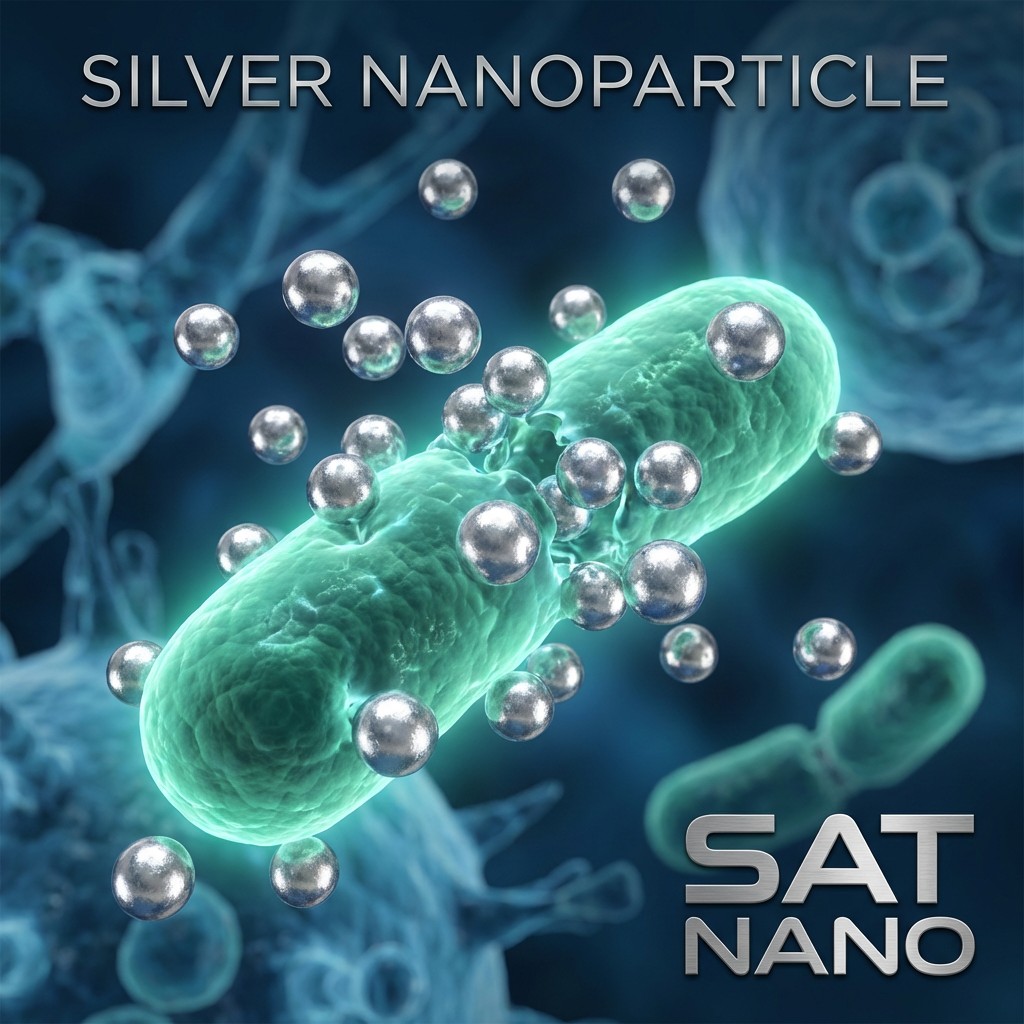
Since ancient times, silver has been widely used for wound treatment and water purification due to its natural antibacterial properties. After entering the nano era, silver nano powder (particle size is usually between 1~100 nm) can release higher concentration of active silver ions (Ag+) due to its extremely high specific surface area, showing far more biological activity than macro silver materials. At present, nanosilver has moved from laboratory research to clinical applications, becoming an important supplement to modern anti infective medical systems.
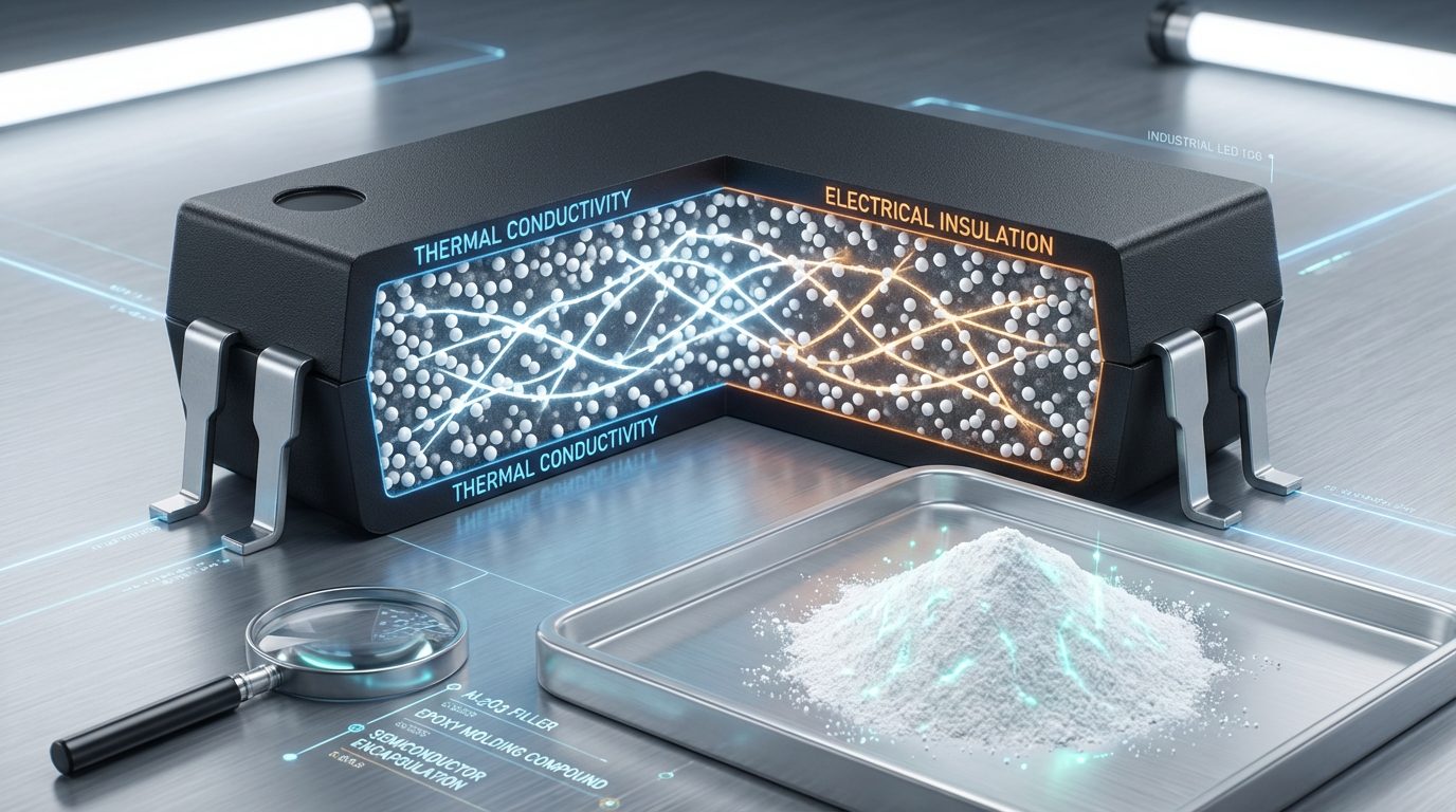
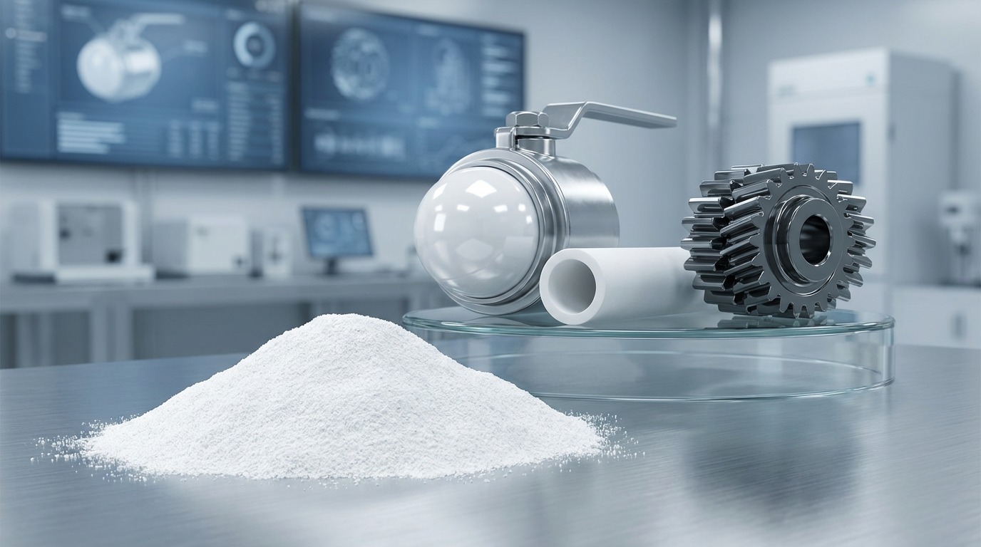
Ultra fine high-purity alumina is a cornerstone material in fields such as electronic information, new energy, high-end manufacturing, and biomedicine. Its application value lies in the precise control of purity, particle size, crystal form, and morphology. Purity determines the upper limit of performance, particle size determines sintering/dispersion/activity, and crystal structure determines functional characteristics. With the development of 5G, solid-state batteries, third-generation semiconductors, and biomedicine, the demand for 6N grade ultra-high purity, monodisperse nanoscale, and spherical alumina will continue to grow. This article discusses the practical applications of ultrafine and high-purity alumina powder.
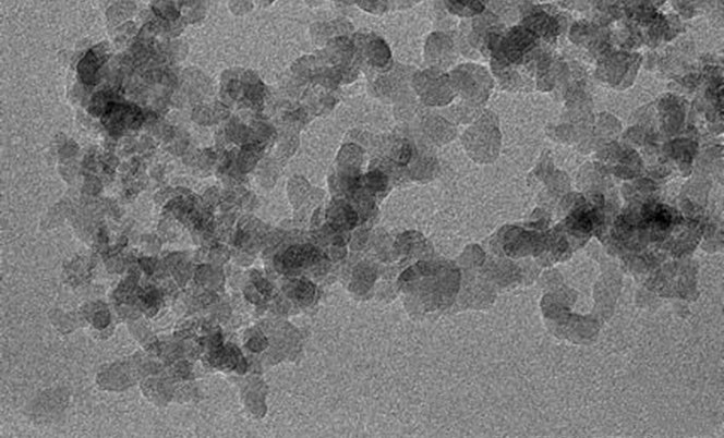
Silicon dioxide SiO2 often has a decisive impact on the performance of systems, whether it is silicone rubber, thin films, or electronic packaging materials.
Scanning Electron Microscope (SEM) is a high-resolution characterization and analysis technique that uses a focused electron beam to scan the surface of a sample point by point, excite secondary electron SE, backscattered electron BSE, characteristic X-rays and other signals, and image them, thereby achieving the microstructure, chemical composition and microstructure of the sample surface. This article will briefly introduce common problems in the SEM testing process, their causes, and corresponding solutions:
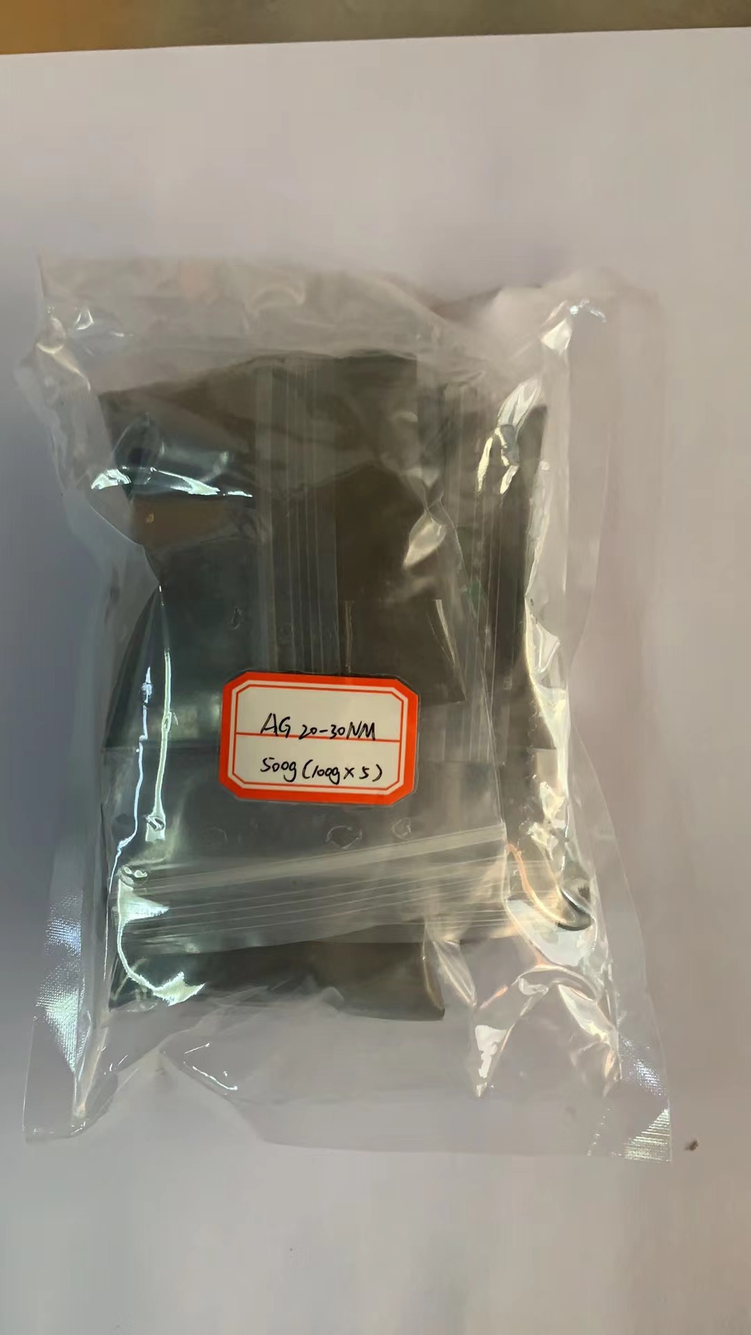
Nano silver powder refers to metallic silver elemental powder with a particle size ranging from 1-100 nanometers (nm), also commonly known as nano silver or silver nanoparticles. Due to its unique physical and chemical properties, it plays a key role in multiple cutting-edge fields such as electronics, medicine, catalysis, and more. The particle size distribution range of nano silver powder is narrow, with commonly used particle sizes of 20nm, 50nm, 80nm, and 100nm. The purity of nano silver powder can reach 99.99%. We can also supply nano silver powder and aqueous dispersion.