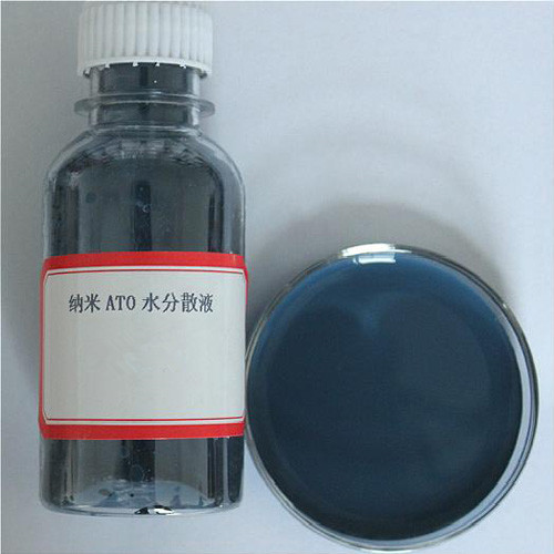
Nanoparticle transmission electron microscopy (TEM) is an important microscopy technique widely used to observe and characterize the structure and morphology of nanoscale particles and materials.
TEM uses high-energy electron beams to observe the microscopic details of the sample through thin slices. In TEM, the electron beam is focused through a lens system and then passes through the sample, interacting with atoms or molecules in the sample. By collecting information on the transmitted electron beam, high-resolution images and diffraction patterns of the sample can be obtained, thereby revealing its internal structure and composition.
The following are the general steps for using TEM to test samples:
1. Sample preparation: Firstly, it is necessary to prepare the sample to be tested into sufficiently thin sample slices. Common preparation methods include mechanical slicing, ion grinding, centrifugal deposition, and focused ion beam (FIB) cutting.
2. Sample loading: Place the prepared sample slices on the TEM sample carrier and ensure their fixation and stability.
3. Instrument settings: Set parameters such as acceleration voltage, focusing, and alignment functions required for TEM. Usually, it is necessary to choose appropriate lens settings and modes to obtain the required image information.
4. Observation and adjustment: Insert the sample holder into the TEM instrument and observe the sample using an eyepiece or microscope. Under appropriate magnification, observe whether the morphology and structure of the sample meet the requirements, and adjust and optimize as needed.
5. Image capture: Select appropriate lens settings and exposure time to capture high-resolution images of the sample through the TEM system. Images from different regions and angles can be collected to obtain more comprehensive information.
6. Data analysis: Analyze and interpret TEM images, including measuring particle size, surface morphology, crystal structure, etc. Corresponding energy spectrum analysis and diffraction pattern analysis can also be conducted to obtain information on elemental composition and crystal structure.
TEM is a high-resolution microscopy technique commonly used to study nanoparticles, nanomaterials, nanostructures, and more. It can provide detailed observation and analysis at the nanoscale, playing an important role in understanding the structural properties of materials, the morphology and composition of nanoparticles, and the study of nanoscale phenomena.


