
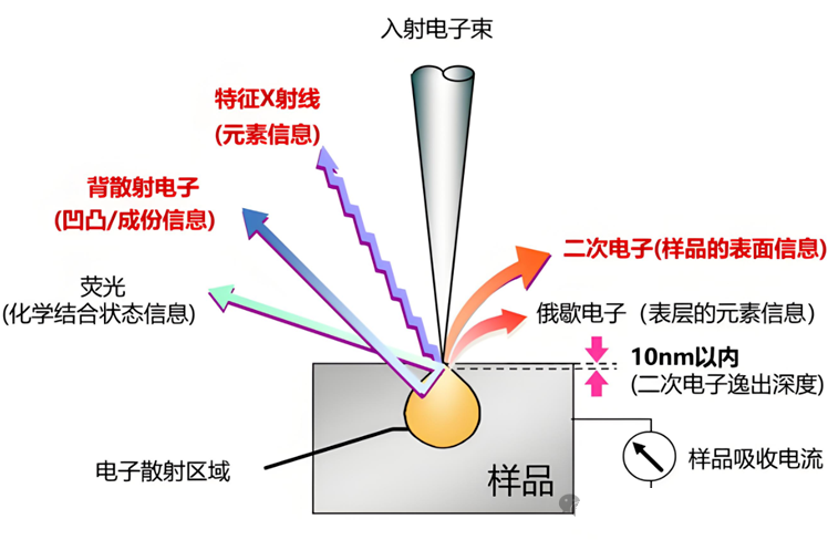
Scanning Electron Microscope (SEM) is a high-resolution characterization and analysis technique that uses a focused electron beam to scan the surface of a sample point by point, excite secondary electron SE, backscattered electron BSE, characteristic X-rays and other signals, and image them, thereby achieving the microstructure, chemical composition and microstructure of the sample surface. This article will briefly introduce common problems in the SEM testing process, their causes, and corresponding solutions:
What can we see through SEM?
SEM can be used for the characterization and analysis of microscopic features of various samples, mainly for the following analyses:
1. Surface microstructure: Secondary electron SE imaging of sample surface morphology, roughness, particle size and distribution, voids, cracks, fracture characteristics, film/coating surface state, etc. are all commonly used functions of SEM;
2. Microstructure and structure: backscattered electron BSE imaging or electron backscatter diffraction EBSD analysis of internal grains, grain boundaries, phase distribution, layered structure, fiber/columnar crystal growth morphology, etc;
3. Elemental composition analysis: Backscattered electron BSE combined with EDS energy spectrometer collects characteristic X-ray imaging for qualitative and semi quantitative analysis of elements in micro areas, and can be combined with secondary electron SE for synchronous analysis of "morphology+composition".

How to conduct SEM testing on non-conductive or poorly conductive samples?
When observing a sample with SEM, the incident electron beam interacts with the sample, causing the accumulation of charges in non-conductive and poorly conductive samples, resulting in a charging effect that affects the observation and shooting of SEM images. To solve this problem, it is necessary to conduct conductive treatment on the sample, that is, by spraying gold or carbon to increase the conductivity of the sample.

Does spraying gold or carbon affect the morphology of the sample?
After gold spraying, the conductivity of the sample will increase, reducing the charge effect and obtaining clearer morphology images. The gold spray layer is generally very thin (at the nanometer level) and does not significantly affect the original morphology of the sample

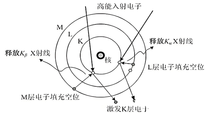
Why can't EDS detect H, He, Li, Be elements?
H. The He element only has K layer electrons, and after being excited by an electron beam, there is no electron backfill, so it will not excite characteristic X-rays; The characteristic X-ray energy of Li and Be elements is lower than the resolution of the energy spectrum, resulting in weak signals and difficult detection.
What is the reason for detecting elements that should not actually exist in the EDS analysis results?
Possible reasons may be that the characteristic X-ray energies of some elements are similar, and EDS cannot distinguish them, resulting in misjudgment in element analysis. For example, the K α peak of S (2.31keV) almost overlaps with the L α peak of Mo (2.29keV). If the sample contains Mo element, it is often misdiagnosed as containing S. In addition, it is also necessary to consider whether the sample is being prepared or contaminated by the environment.
Why can't SEM-EDS accurately perform quantitative analysis?
1. The limitation of the detection principle is that EDS determines the type of element and estimates its content by detecting the characteristic X-ray energy and intensity emitted by the sample after being excited by an electron beam. However, the X-ray intensity is influenced by various factors such as sample morphology, inter element absorption effects, instrument conditions, etc., resulting in errors in quantitative results.
2. Quantitative analysis of standard dependence and calibration limitations requires the use of standard samples with similar components to the sample being tested for calibration, but actual samples may not fully match the standard conditions (such as non-uniform, multiphase materials). High precision can be achieved for heavy elements (such as metals and rare earths) through standard sample correction, while for light elements (such as B, C, N), the error significantly increases due to low X-ray yield. Therefore, semi quantitative SEM-EDS is only suitable for rapid component screening, but high-precision quantification requires the combination of other techniques.
SAT NANO not only provides high-quality products, but also offers one-stop services for sample preparation, electron microscopy characterization, and data analysis. If you have any enquiry, please feel free to contact us at sales03@satnano.com