

Transmission electron microscopy (TEM) is an indispensable research tool in fields such as materials science and nanotechnology. For researchers who are new to TEM, understanding its basic principles and operations is crucial for efficient utilization of this equipment. TEM testing mainly focuses on the microstructure characteristics of materials, including element distribution, phase composition, crystal defects, etc. These characteristics are manifested at the microscopic level as the size, shape, distribution of different phase grains, as well as the density and distribution of crystal defects. Through TEM, researchers can gain a deeper understanding of the internal structure of materials, thereby evaluating their properties and potential applications.
Compared with other analytical instruments such as spectrometers, X-ray diffractometers, etc., the biggest advantage of TEM is its ultra-high spatial resolution. TEM can not only detect the elemental composition of materials, but also analyze the crystal structure at the atomic level, achieving in-situ observation. This ability makes TEM an irreplaceable tool in nanoscale research. As a third-party testing and analysis institution that provides testing, identification, certification, and research and development services, Jinjian Laboratory not only has a professional technical team, but also is equipped with advanced testing equipment to provide you with accurate TEM testing services.
The reason why TEM can achieve atomic level high resolution is because it uses a high-speed electron beam with extremely short wavelength as the illumination source. The resolution of ordinary optical microscopes is limited by the wavelength of the illumination beam, while the wavelength of the electron beam is much shorter than visible light, so the resolution of TEM is much higher than that of traditional microscopes. In addition, the wave particle duality of electron beams enables TEM to achieve atomic level imaging of materials.
The basic structure and function of TEM
The basic structure of TEM includes key components such as electron gun, condenser, sample stage, objective lens, intermediate mirror, and projection mirror. The electron gun generates a high-speed electron beam, which is focused by a condenser lens. The sample stage carries and precisely positions the sample, and the objective lens and intermediate mirror further magnify the image of the sample. The projection mirror projects the magnified image onto a fluorescent screen or detector. The collaborative work of these components enables TEM to achieve high magnification imaging and analysis of samples.
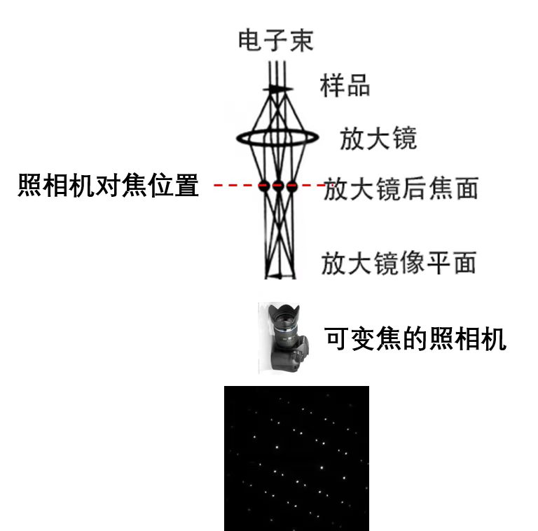
TEM mainly has three working modes: magnification imaging mode, electron diffraction mode, and scanning transmission mode (STEM). In magnification imaging mode, TEM is similar to traditional optical microscopes to obtain the morphology image of the sample; In electron diffraction mode, TEM captures the diffraction pattern of the sample, reflecting its crystal structure; In STEM mode, TEM scans the sample point by point by focusing the electron beam, and collects signals with a detector to achieve higher resolution imaging.
Differences in TEM imaging: bright field image, dark field image, central dark field image
Bright field image: Only allows the transmitted beam to pass through the objective aperture for imaging, displaying the overall structure of the sample.
Dark field image and central dark field image: Specific diffraction beams pass through the objective aperture, and the central dark field image emphasizes the imaging of the diffraction beam along the transmission axis direction, usually with better imaging quality.
The aberrations of TEM are the main factors limiting the resolution of electron microscopes, including spherical aberration, chromatic aberration, and astigmatism. Spherical aberration is caused by the difference in refractive power of electrons in the center and edge regions of a magnetic lens, chromatic aberration is due to the dispersion of electron energy, and astigmatism is caused by the non axisymmetric nature of the magnetic field. The diffraction difference is caused by the Fraunhofer diffraction effect at the aperture.
Contrast type of TEM
The contrast of TEM is caused by scattering generated by the interaction between electrons and matter, including thickness contrast, diffraction contrast, phase contrast, and Z-contrast. Thickness contrast: Reflecting the surface characteristics and morphological features of the sample, caused by the differences in atomic number and thickness of different micro regions of the sample. Diffraction contrast: Due to the different crystallographic orientations within the sample, which conform to different Bragg conditions, the diffraction intensity varies from place to place. Phase contrast: When the sample is thin enough, the phase difference of the electron beam wave penetrating the sample produces contrast, which is suitable for high-resolution imaging. Z-contrast: In STEM mode, image brightness is proportional to the square of atomic number and is suitable for observing element distribution. By mastering these fundamental knowledge, TEM users can more effectively utilize this tool for microstructure analysis of materials.
SAT NANO is a best supplier of nanoparticle and micro particle in China, we can offer metal powder, carbide powder, oxide powder and alloy powder, if you have any enquiry, please feel free to contact us at sales03@satnano.com